BQ77915 Battery Management System (BMS) Schematic Design and Component Selection
This video, part 4 of the BMS Design Series, focuses on creating a functional schematic for a 5-series lithium-ion Battery Management System using the BQ77915 chipset. The speaker emphasizes designing a BMS based on its architecture and functionality, rather than general schematic drawing tutorials. Key components are selected, including the BQ77915 non-smart chipset (chosen for cost-effectiveness), a 1.5 milliohm current sense resistor for 20A continuous and 46A pulse current, and AON6144 FETs for their low on-resistance and voltage tolerance. Detailed calculations and considerations derived from the datasheet are crucial for each component. The design incorporates features like internal cell balancing, overcurrent protection (23A continuous, 46A pulse), and short-circuit protection (120A spike within 960µs). The speaker demonstrates the practical steps of laying out the schematic in Altium Designer, including connecting cell inputs, configuring power lines, and setting up FET drive circuitry, ensuring proper connections and stable operation. The video highlights the importance of precise component selection (e.g., 1% resistors) and adherence to industry best practices like Kelvin connections for current sensing and avoiding quad junctions in schematics.

Introduction & Objectives [0:00]
The video initiates Part 4 of a Battery Management System (BMS) design series, focusing on the creation of a schematic.
- Purpose of the video: To teach BMS architecture and system design rather than general schematic or Altium software tutorials.

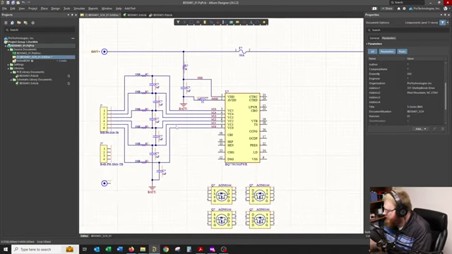
Altium Designer Interface with BQ77915 Component [ 00:01:26 ] - Live stream format: The content is presented as a live stream to allow for real-time interaction and questions from viewers.
Component Selection & Calculations [1:33]
The initial step in BMS design is to select critical components, starting with the chipset.
- Chipset Selection: BQ77915 [1:43]
- Type: A non-smart, or "dumb," chipset is chosen, meaning it has pre-programmed settings and cannot be programmed via software like smart chips (e.g., BQ40Z50, 40Z80).
- Configuration: Settings for overvoltage, undervoltage, overcurrent, short-circuit, and temperature are selected from a fixed table (e.g., 1501 SKU chosen for 4.25V overvoltage and 2.8V undervoltage thresholds).

BQ77915 Device Comparison Table with Pre-Programmed Values [ 00:03:30 ] - Cost-effectiveness: Non-smart chips are significantly cheaper ($1 vs $2-3 for smart chips in large quantities), making them ideal for high-volume production if specific parameters are acceptable.
- Current Sense Resistor Calculation [5:40]
- Principle: The BMS measures voltage drop across a current sense resistor to determine current. The chip's thresholds (e.g., 35mV for overcurrent discharge 1, 60mV for overcurrent discharge 2) are hardware-set.
- Calculation:
- For a 20A continuous current and a 35mV threshold, a 1.75 milliohm resistor is needed (35mV / 20A).
- A more common 1.5 milliohm resistor is selected, resulting in a 23.33A trip point for overcurrent discharge 1 and 46.66A for overcurrent discharge 2 (which is double the first threshold).
- Decision: A 1.5 milliohm current sense resistor is noted for the schematic.
- FET Selection: AON6144 [8:11]
- Criteria:
- Low on-resistance: Minimizes voltage drop and heat dissipation for continuous current (20A).
- Voltage tolerance: Must be sufficient for the pack voltage (e.g., 40V FET for a 21V pack).
- Gate-to-Source Voltage: Ensure the BMS chip can properly drive the FETs into full conduction.
- Short-circuit Current Handling: FETs must tolerate high current spikes (e.g., 120A for the P26A cell) and cut off within specified times (e.g., 960µs). The AON6144 is suitable for this, preventing "burning up" during hard current stops.
- Quantity: Two pairs of FETs are used to enhance continuous and short-circuit current handling.
- Criteria:
- Fuse Selection: A standard 30A off-the-shelf fuse is chosen.
Datasheet Navigation & Key Parameters [11:00]
The presenter emphasizes the critical importance of reading the full datasheet for any component.
- Pin Functions [11:12]: Provides information on how to use or terminate unused pins.
- Absolute Maximum Ratings [11:27]: Details the maximum allowable voltages for inputs (36V), sense pins (3.6V), and outputs (20V).

BQ77915 Electrical Characteristics Table [ 00:16:14 ] - Recommended Operating Conditions [12:35]: Lists typical operating currents (80-115 µA in normal mode, 3 µA in hibernate, 500 nA in shutdown).
- Device Configuration Table [14:00]: Explains that different SKUs of the chip (e.g., -01, -02, -04) have different pre-programmed voltage, current, and temperature thresholds, which cannot be changed by the user. Texas Instruments offers custom SKUs for high-volume orders.
- Overcurrent Discharge Programming [22:06]: While internal thresholds are fixed, the delay options for overcurrent discharge 1 (OCD1) and 2 (OCD2) can be programmed externally using a resistor on the OCDP pin.
- A 750kΩ resistor is selected for the OCDP pin to achieve the longest possible delays: 1420ms for OCD1 (23A threshold) and 700ms for OCD2 (46A threshold), ensuring the higher current pulse has a shorter trip time.

Overcurrent Discharge Programming Table with Timing Values [ 00:23:30 ]
- A 750kΩ resistor is selected for the OCDP pin to achieve the longest possible delays: 1420ms for OCD1 (23A threshold) and 700ms for OCD2 (46A threshold), ensuring the higher current pulse has a shorter trip time.
Understanding Chipset Functionality & Modes [19:51]
The video delves into specific functional aspects and operational modes of the BQ77915.
- Protection Summary [20:20]: Two internal comparators manage voltage (OV, UV) and current (OCD, SCD, OC) protections.

State Comparator Summary in Fault Conditions [ 00:51:23 ] - Recovery Options [20:50]: Explains how the BMS recovers from fault conditions (e.g., load removal or time expiration) and emphasizes the importance of avoiding constant short-circuit attempts that can degrade MOSFETs.
- Temperature Protection [29:55]: Discussion on how the chip operates under various temperature conditions (overtemperature/undertemperature in charge/discharge).

BQ77915 Operation in OTC/OTD/UTC/UTD Tables [ 00:32:05 ] - Cell Balancing [35:26]:
- Internal vs. External: The chip supports both internal and external cell balancing. Internal balancing is used in this design.
- Activation: Cell balancing is enabled by connecting the CB1 pin to VSS. Leaving it floating disables balancing.
- Current Control: The R_INI series resistors on the cell inputs control the balancing current. A value of 100 ohms is chosen to provide approximately 35mA of balancing current (based on a 3.8V cell balance turn-on threshold).

Cell Balancing Algorithm Explanation [ 00:38:31 ] 
Cell Balancing with External MOSFETs Application [ 00:44:37 ]
- Stacking Implementation (Viewer Question) [13:39]:
- Concept: Multiple BQ77915 chips can be stacked to manage higher cell count battery packs (from 3 to 20+ series). The ground reference of an upper chip connects to the positive terminal of the cell monitored by the chip below it.
- Design Consideration: Series diodes are crucial between stacked chips to prevent reverse current flow and voltage potential issues, especially when switching.

BQ77915 10-Series Configuration with Internal Cell Balancing [ 00:14:00 ]
- Device Functional Modes [55:48]:
- Power-On Reset: The chip performs self-checks during boot-up.
- Normal Mode: Charge and discharge are enabled, and cell balancing can occur.
- Fault Mode: Triggered by comparator circuits; turns off charge/discharge FETs until recovery.
- Hibernate Mode: Low-power mode, activated by driving the System Present (PRES) pin high. This allows the battery pack to be "turned off" to prevent draining when idle.
- Shutdown Mode: Occurs when cell voltage drops below a critical threshold, completely disabling output for safety.

BQ77915 Device Operational States Flowchart [ 00:59:08 ]
- Customer Fast Protection Test Modes [59:31]: A unique feature that allows rapid testing of fault conditions by overriding recovery times. This speeds up manufacturing test processes by quickly cycling through protection triggers.
- Charge/Discharge FET Protection [1:07:09]: Explains the need for proper gate drive resistors and pull-down resistors to ensure FETs turn off quickly under high current conditions, preventing degradation. A Zener diode can be used across the FET gate-source to protect against overvoltage.

Recommended System Implementation of FETs [ 01:07:14 ] - Load Detection (LD) [1:11:33]: The LD pin detects if a load is connected to the battery output. This prevents auto-recovery from certain faults (e.g., undervoltage, overcurrent in discharge) until the load is removed, ensuring safety and preventing rapid cycling.
Schematic Design Process in Altium [1:20:30]
The video transitions to the practical implementation of the schematic in Altium Designer.
- Software: Altium Designer is used, leveraging its manufacturer part search feature for component data.
- Real-world Example [1:26:37]: The speaker demonstrates a physical battery pack with a custom BMS designed by their team.

Speaker showing a real-world battery pack with BMS [ 00:26:59 ] - General Layout Principles: Emphasizes neatness, clear organization (power flowing one way, signals another), and avoidance of "quad junctions" (where four wires meet at one point) for clarity and to prevent software interpretation errors.
- Main Components Placement:
- BQ77915 chipset is placed centrally.
- Input connector for cell sense lines.
- Four AON6144 FETs (two for charge, two for discharge) are placed.
- Output pads and fuse.
- Connectors for system present switch and thermistors for an external charger.

BQ77915EVM Schematic as Design Reference [ 01:21:42 ]
- Cell Input Connections [1:31:50]:
- Six-pin JST connector for 5-series battery input.
- Each cell input includes a 100-ohm series resistor and a 1µF capacitor to ground or between cell lines (VC pins).
- Illustrates how to avoid quad junctions in wiring for clarity.

Initial Cell Input Connections Avoiding Quad Junctions [ 01:33:34 ] 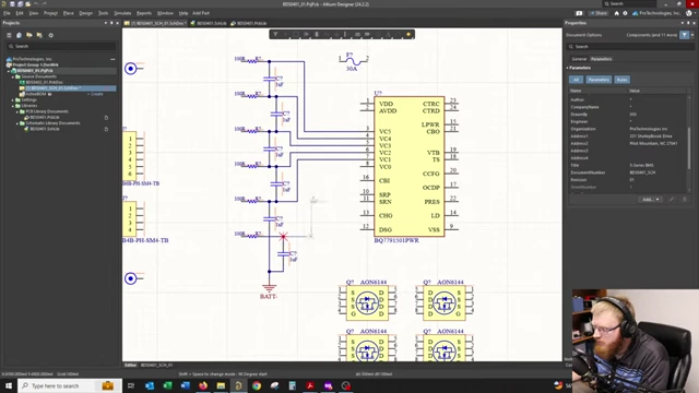
Completed Cell Input Connections with Net Labels [ 01:37:07 ]
- Power Line Connections (VDD, AVDD) [1:42:45]:
- Current Sense Resistor Circuit [1:51:14]:
- 1.5 milliohm current sense resistor is placed.
- A common filter circuit is implemented with two 0.1µF capacitors to ground and one 0.1µF capacitor across the SRP/SRN lines.
- Kelvin Connections: Stress is placed on making very short, direct connections from the SRP/SRN pins to the pads of the current sense resistor to maintain accuracy.
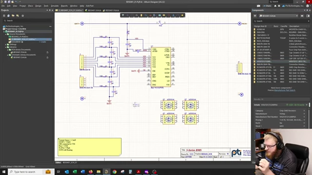
Current Sense Resistor Placement [ 01:51:15 ] 
Kelvin Connection Setup for Current Sensing [ 01:53:33 ]
- FET Drive Circuitry [2:01:10]:
- Initial FET Placement: FETs connected to the current sense resistor.

Charge/Discharge FETs and Current Sense Connection [ 01:58:18 ] - Discharge FETs: Driven by the DSG pin through a 5.1kΩ series resistor and a 1MΩ pull-down resistor. Additional 51Ω resistors are added for each FET when paralleling to prevent ringing.
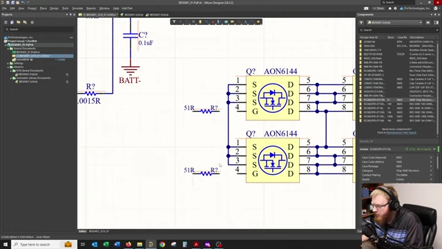
Discharge FETs with Individual Gate Resistors [ 02:01:52 ] 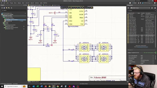
Discharge FET Path to Current Sense Resistor [ 02:02:53 ] - Charge FETs: Driven by the CHG pin through a 5.1kΩ series resistor, a 3MΩ pull-down resistor, and protected by a 16V Zener diode (value chosen from evaluation module).
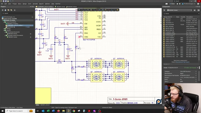
Initial Charge FET Drive Connections [ 02:05:23 ] 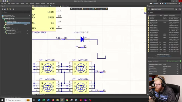
Charge FET Drive with Diode Protection [ 02:08:11 ] - Complete FET Drive: Shows the entire arrangement of charge and discharge FETs with their respective gate drives and protection.

Complete Charge/Discharge FET Drive Circuitry [ 02:16:21 ]
- Initial FET Placement: FETs connected to the current sense resistor.
- Control Pin Connections:
- VSS: Directly tied to battery ground.
- Load Detection (LD): Connected to
pack-via a 47kΩ resistor to detect load removal for fault recovery.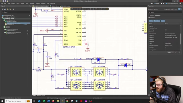
VSS and Load Detection Pin Connections [ 02:18:20 ] 
Load Detection Connection to Output [ 02:21:00 ] - OCDP: Connected to
batt-via a 750kΩ resistor for the calculated overcurrent discharge delay. - PRES: Connected to
pack+via a 10kΩ pull-up resistor for an external power switch.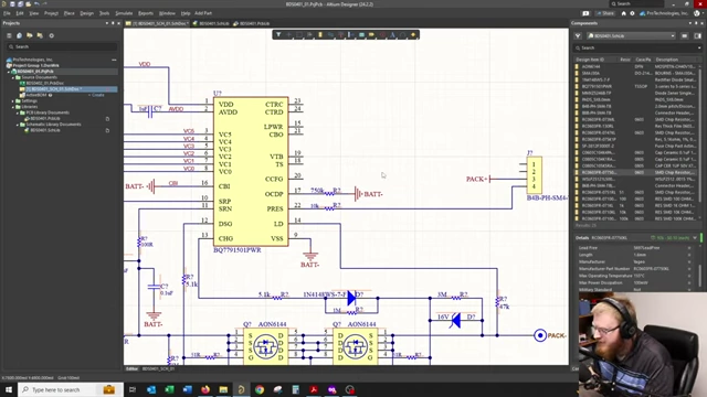
OCDP and Thermistor Sensor (TS) Pin Connections [ 02:27:10 ] - TS: Connected to
VTB(highest cell voltage reference) via a 10kΩ resistor, with its output tied to an external thermistor connector for charger communication.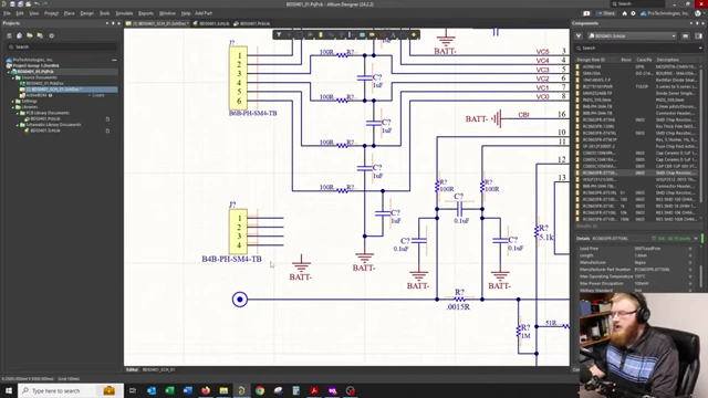
External Thermistor Connections on the Schematic [ 02:29:03 ] 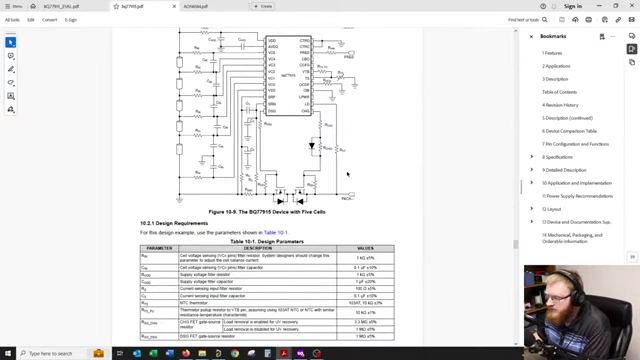
Simplified Schematic with Design Parameters [ 02:30:22 ] - CCFG: Left floating to configure the chip for 5-series operation.
- LPWR & CBO: Left floating as they are for stacking implementations which are not used in this single-chip design.
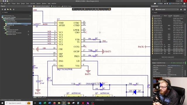
CBO and LPWR Pins Handled by "No ERC" Directives [ 02:32:27 ] - CTR_C & CTR_D: Connected directly to ground as stacking is not being used.
- Final Touches & Annotation [2:33:30]:
- Additional 0.1µF capacitors are placed between the output terminals for stability and between FET drains and sources to prevent ringing.
- The schematic is then automatically annotated, assigning unique designators (e.g., R1, C1, D1) to all components.
- The completed schematic provides a 5-series BMS capable of handling up to 23A continuous current with 46A spikes, two thermistors, and a power on/off switch.