Rapid PCB Prototyping with VIA Grid: Laser Etching Pre-Fabricated Double-Sided Boards in 90 Minutes
- The video introduces "VIA Grid," a standardized PCB blank with pre-baked vias, designed for ultra-rapid prototyping of double-sided PCBs.
- It solves the traditional difficulty and time-consuming nature of making vias, which usually involves chemicals or manual rivet installation.
- The process involves designing a schematic, importing it into a VIA Grid template, and then laser etching the traces on both sides using a DPSS UV laser like the Commarker Omni 1.
- With the aid of a LumenPnP pick-and-place machine, paste extruder, and reflow oven, a complete functional PCB can be produced from design to assembly in under 90 minutes.
- A custom alignment jig ensures consistent and precise laser etching, making the process reliable and repeatable.
- All design files, settings, and the jig design are open-sourced on GitHub, encouraging community collaboration to develop this rapid prototyping method further.
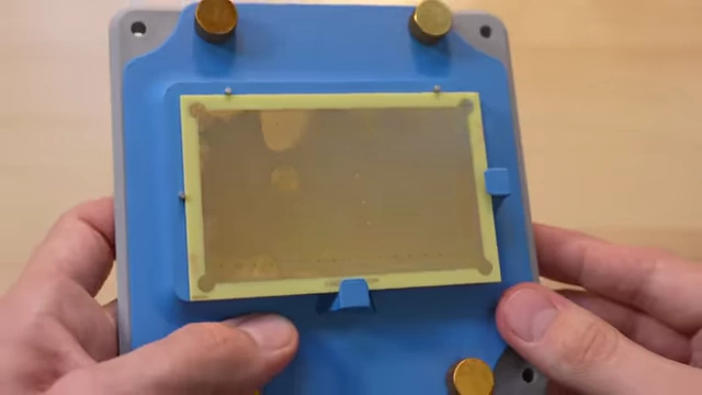
A finished VIA Grid standardized PCB blank [ 00:00:40 ]
The Challenge of PCB Vias and the VIA Grid Solution [00:00:00]
Making vias (vertical interconnect access) for rapid PCB prototyping has traditionally been difficult and time-consuming, involving:
- Complex chemical processes like acid baths and electroplating

Chemical process for making vias at home, involving multiple hazardous steps [ 00:00:11 ] - Manual installation of large rivets that are not suitable for dense ICs

A small rivet held by tweezers, illustrating the manual installation required for traditional vias [ 00:00:16 ]
The VIA Grid concept proposes a solution:
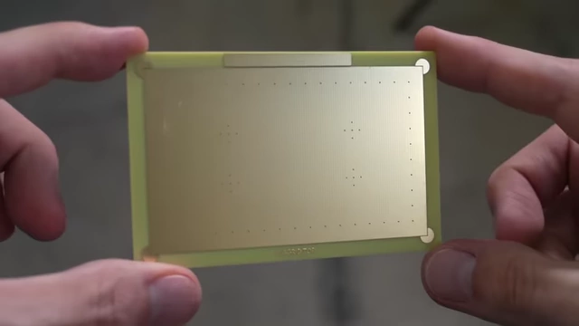
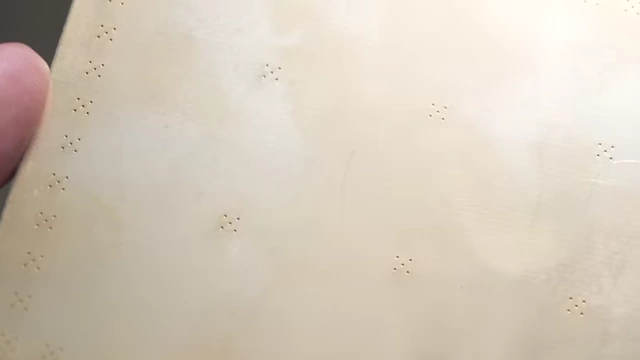
- Using a standardized PCB blank with a pre-baked array of factory-made vias
A blank VIA Grid PCB with a pre-baked array of vias [ 00:00:26 ] - This eliminates the need to create vias in a home setting, leveraging the efficiency of professional board shops
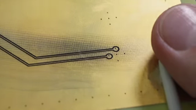
- The user simply defines which vias are connected when etching traces on the front and back sides
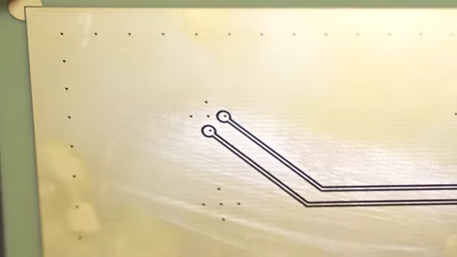
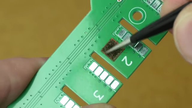
Laser-etched traces connecting to pre-baked vias on a VIA Grid PCB [ 00:00:29 ]
- This method enables rapid prototyping, completing a functional double-sided PCB in under an hour for etching and under 90 minutes for the entire assembly process
A finished VIA Grid standardized PCB blank [ 00:00:40 ]
The Rapid Prototyping Process [00:00:45]
The VIA Grid method streamlines PCB creation from design to functional board.
1. Design and Layout [00:00:45]
- Design the schematic as usual
- Drop the design into a VIA Grid template PCB in your EDA software (e.g., KiCad)
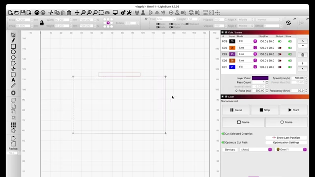
2. Laser Etching [00:00:59]
- Export the design and load it into LightBurn software
- Use a DPSS (Diode Pump Solid State) UV laser to etch the copper traces
3. Assembly [00:01:07]
- Couple the etched PCB with:
- A LumenPnP pick-and-place machine
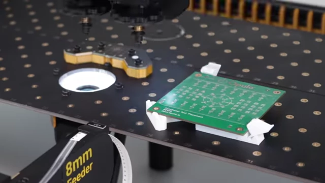
LumenPnP pick and place machine assembling components onto the etched PCB [ 00:01:10 ] - A paste extruder for solder paste application
Solder paste being applied by a paste extruder on the pick-and-place machine [ 00:01:10 ] - A reflow oven for soldering components
A reflow oven used for soldering components onto the PCB [ 00:01:11 ]
- A LumenPnP pick-and-place machine
- The entire process, from design to a finished, functional double-sided board, can be completed in under 90 minutes
A completed PCB being assembled by the LumenPnP machine [ 00:01:15 ]
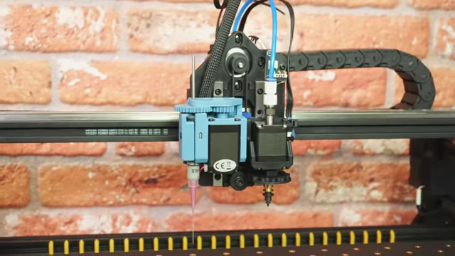
Advanced Laser Technology for PCB Etching [00:01:27]
Traditional fiber lasers have limitations for PCB etching.
- Fiber lasers make FR4 (standard PCB substrate) conductive when cutting, requiring the use of less common FR1 substrates
Close-up showing conductive residue left on FR4 by a fiber laser, causing shorts [ 00:01:35 ]
The solution involves using DPSS UV lasers:
- These lasers use UV light and do not burn materials, preventing FR4 from becoming conductive
- The Commarker Omni 1 is an example of a commercially available DPSS laser at a reasonable price point
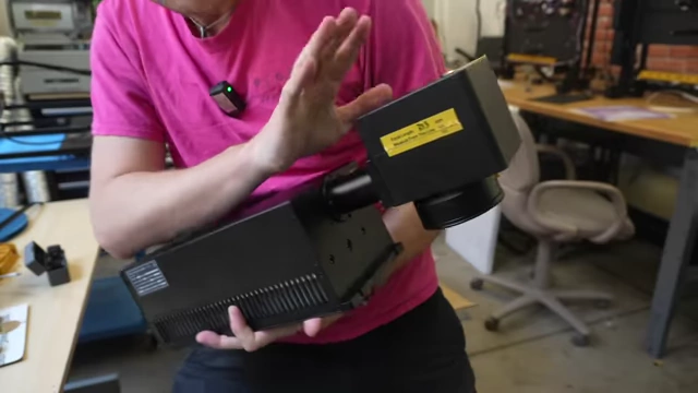
The Commarker Omni 1 DPSS UV laser held by the speaker [ 00:01:40 ] - A new enclosed version (Commarker Omni X) offers improved safety features like ventilation and interlocks
- Achieving precise etching requires extensive tuning of laser settings (power, speed, frequency)
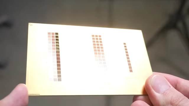
Test patterns showing different laser settings for etching on a PCB blank [ 00:02:36 ] - A custom LightBurn project file with optimized settings and alignment features is provided to simplify future use
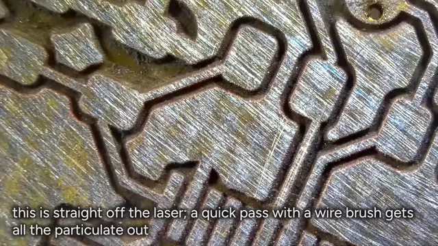
Macro view of finely etched copper traces after a quick clean [ 00:02:47 ] 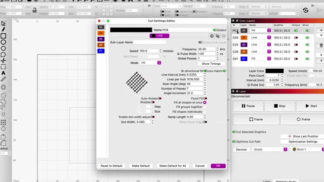
LightBurn software interface displaying optimized laser settings for PCB etching [ 00:02:56 ] 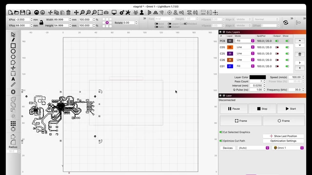
LightBurn software interface with a PCB design loaded, ready for laser etching [ 00:03:00 ]
- A custom LightBurn project file with optimized settings and alignment features is provided to simplify future use
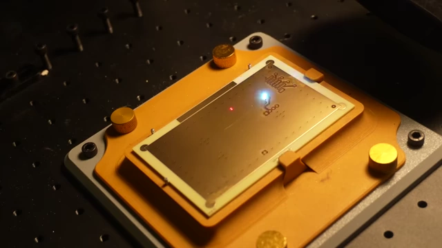
Precision Alignment System and Jig [00:03:01]
Accurate alignment of the PCB with the laser is crucial for VIA Grid.
Initial attempts at software-based alignment were tedious and imprecise
A key discovery was that the laser is nearly invisible on the ENIG plating but lights up brightly on the exposed FR4 substrate
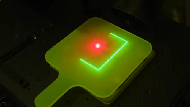
Laser light outlining the PCB area on a test paddle, showing how the laser becomes visible on FR4 [ 00:03:23 ] Alignment Features ("Pac-Man" features):
- VIA Grid PCBs are designed with small "Pac-Man" shaped features in the corners, exposing a slim path of fiberglass
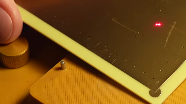
Laser light illuminating the exposed fiberglass alignment features on the PCB [ 00:03:30 ] 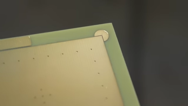
Close-up of the "Pac-Man" alignment features in the corner of a VIA Grid PCB [ 00:03:34 ] - When LightBurn's "frame" function is used at low power, these features light up perfectly when the board is aligned and scaled correctly
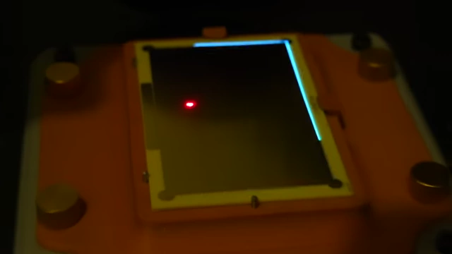
Laser highlighting the "Pac-Man" alignment features on the PCB for precise positioning [ 00:03:43 ]
- VIA Grid PCBs are designed with small "Pac-Man" shaped features in the corners, exposing a slim path of fiberglass
Custom Alignment Jig:
- A two-plate jig was developed for consistent physical alignment
- The bottom plate bolts to the laser base
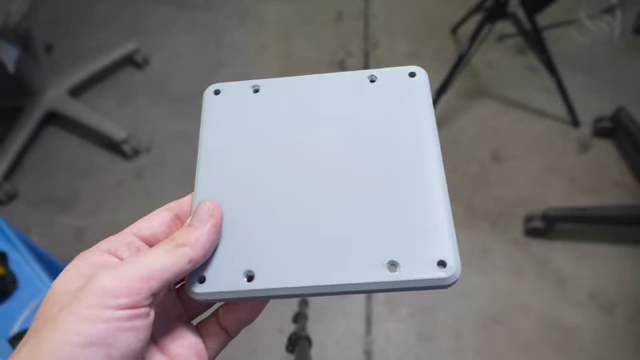
The bottom plate of the custom alignment jig [ 00:03:51 ] - The top plate holds the PCB using three dowel pins and two spring-loaded cams for consistent re-indexing
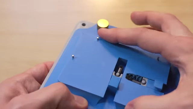
Custom two-plate alignment jig with PCB in place, showing dowel pins and spring-loaded cams [ 00:03:55 ] - The top plate is attached with four loose thumb screws, allowing for minor adjustments until the corner "Pac-Man" features align perfectly, then tightened
The alignment jig securely holding a VIA Grid PCB [ 00:04:00 ] 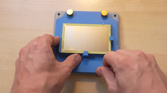
Adjusting the top plate of the alignment jig to precisely align the PCB [ 00:04:05 ]
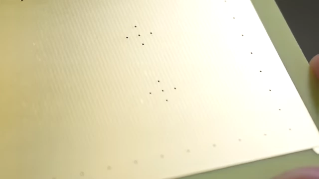
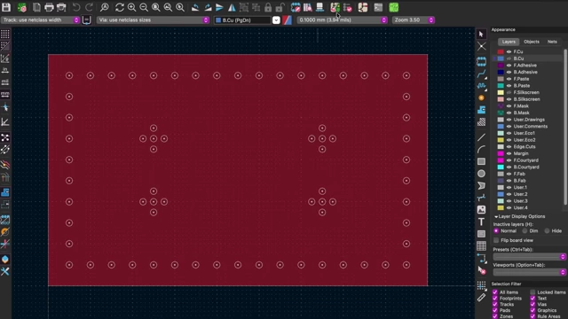
Via Arrangement and Future Possibilities [00:04:27]
Optimizing the via layout on the VIA Grid was an iterative process.
- Initial designs used tiny, densely packed via clusters
Previous VIA Grid design with densely packed via clusters at the edges and in pockets [ 00:04:37 ] - This resulted in an excessive number of vias and made alignment significantly more difficult
- The improved design spaces out the vias considerably
- This creates a more forgiving layout, ensuring connections even if alignment isn't absolutely perfect
Improved via layout with wider spacing for easier routing and alignment [ 00:04:50 ] - The increased spacing did not negatively impact usability
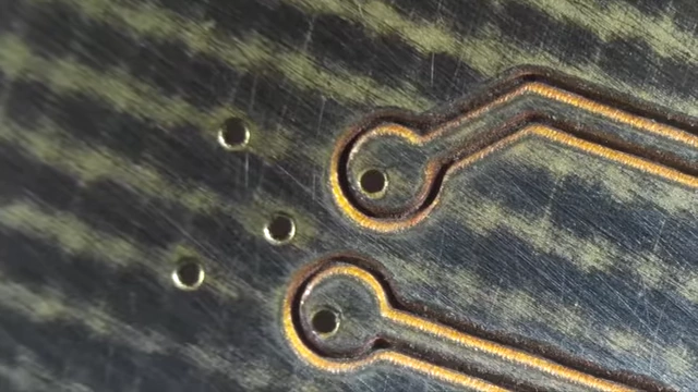
Close-up of the improved via layout with wider spacing on a VIA Grid PCB [ 00:04:57 ]
- This creates a more forgiving layout, ensuring connections even if alignment isn't absolutely perfect
4-Layer Board Concept [00:05:01]
- The presenter explored the potential for a 4-layer board using this method
- Inner layers would be dedicated to fixed nets like power or ground planes
- Specific vias would connect to inner layer 1 (e.g., power) and others to inner layer 2 (e.g., ground)
Conceptual design for a 4-layer VIA Grid board with dedicated ground planes [ 00:05:10 ]
- Specific vias would connect to inner layer 1 (e.g., power) and others to inner layer 2 (e.g., ground)
- This allows for even power/ground distribution but requires etching to isolate unused vias
- This will add some etching time, but it's not much for the benefit gained.
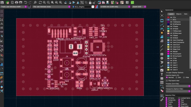
Real-World Application and Future Vision [00:05:30]
VIA Grid has already demonstrated significant impact.
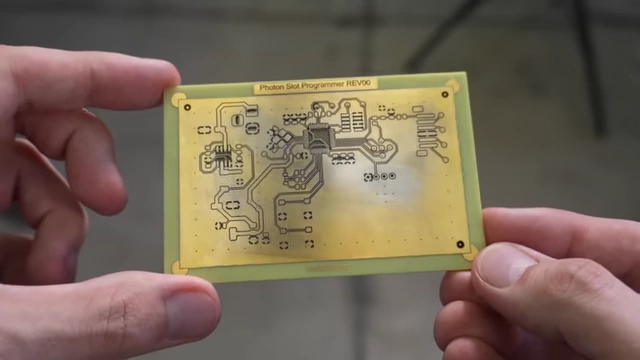
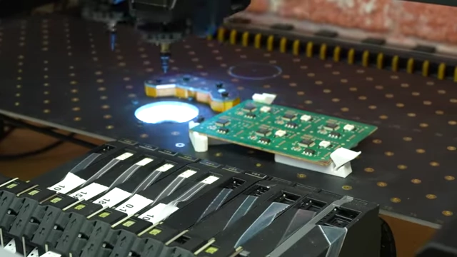
- A complex feeder PCB (a component shipped in thousands) was redesigned using VIA Grid
An older, prototype feeder jig used for programming feeder slots for pick-and-place machines [ 00:05:41 ] - Layout took only 20 minutes
- A fully finished PCB was ready in a couple of hours
New PCB layout for the feeder jig designed on a VIA Grid template [ 00:05:50 ]
- The laser can also drill holes for through-hole components, such as barrel jacks, directly into the PCB
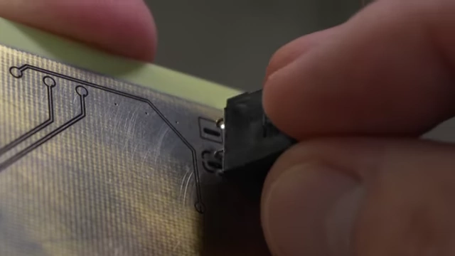
A through-hole barrel jack being inserted into a laser-drilled hole on the PCB [ 00:06:14 ]
The speaker believes this heralds a new wave of hardware prototyping:
- Engineering companies could have dedicated workbenches for 90-minute PCB prototyping, similar to the widespread adoption of 3D printers

A functional PCB with an LED illuminated, demonstrating a successful prototype [ 00:06:36 ] - The process can also include applying solder mask for more professional-looking boards.
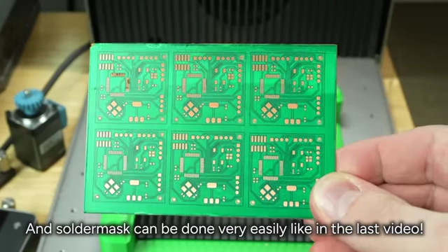
An example of a PCB with applied solder mask layer [ 00:06:40 ] - This requires design concessions, primarily board size and via placement, but otherwise offers true design freedom
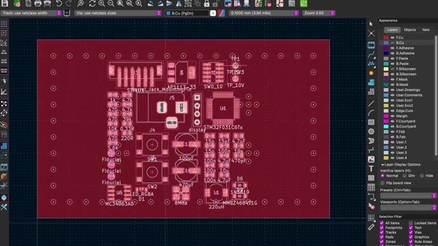
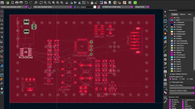
A KiCad layout with traces and vias, demonstrating design flexibility within the VIA Grid standard [ 00:07:10 ] - The project encourages community collaboration, with all files (LightBurn project, VIA Grid PCB design, design rules, KiCad template, jig design) available on GitHub
LightBurn software displaying the PCB settings for the VIA Grid project [ 00:07:18 ] 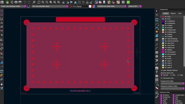
The KiCad design file for the VIA Grid PCB blank [ 00:07:20 ] 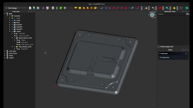
A 3D CAD model of the alignment jig for the laser etching process [ 00:07:28 ] 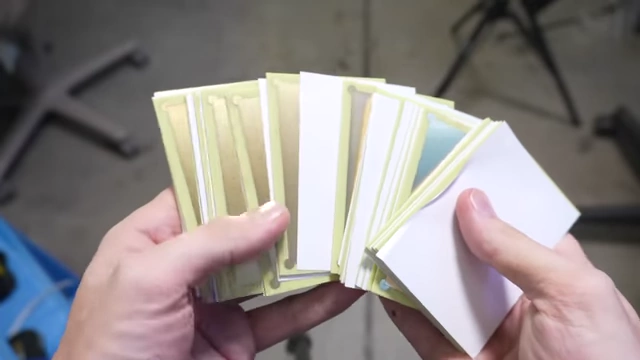
A stack of VIA Grid standardized PCB blanks ready for use [ 00:07:33 ]
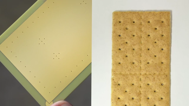
The speaker is seeking feedback and suggestions for a new name for the "VIA Grid" standard, noting its current name was chosen randomly and the via layout resembles a graham cracker.